OPTEK Technology Inc. 1645 Wallace Drive, Carrollton, Texas 75006
Phone: (972) 323-2200 or (800) 341-4747 FAX: (972) 323-2396 sensors@optekinc.com www.optekinc.com
Issue A.2 04/09
Page 5 of 8
Photologic?Slotted Optical Switch
OPB615, OPB616, OPB617, OPB618 Series
OPB625, OPB626, OPB627, OPB628 Series
OPB665, OPB666, OPB667, OPB668 (N and T Series)
OPTEK reserves the right to make changes at any time in order to improve design and to supply the best product possible.
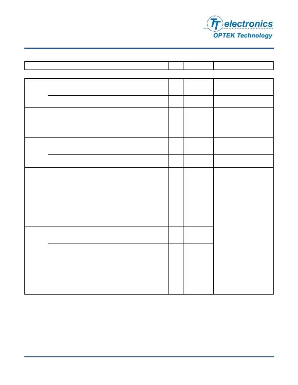
Electrical Characteristics (T
A
= 25癈 unless otherwise noted)
SYMBOL
PARAMETER
MIN TYP MAX UNITS
TEST CONDITIONS
Output Photologic?Sensor
High Level Supply Current:
Buffer, 10k Pull-up
OPB615, 625, 665
Buffer, Open-Collector
OPB616, 626, 666
-
-
5
5
12
12
mA NO LOAD on Output
(3)
Inverted, 10k Pull-up
OPB617, 627, 667
Inverted, Open-Collector
OPB618, 628, 668
-
-
4
4
12
12
mA
NO LOAD on Output
I
F
= 0 mA
I
CCL
Low Level Supply Current:
Buffer, 10k Pull-up
OPB615, 625, 665
Buffer, Open-Collector
OPB616, 626, 666
-
-
5.5
4.0
12
12
mA
NO LOAD on Output
I
F
= 0 mA
Inverted, 10k Pull-up
OPB617, 627, 667
Inverted, Open-Collector
OPB618, 628, 668
-
-
6.5
5.0
12
12
mA
NO LOAD on Output
(3)
V
OH
High Level Output Voltage:
Buffer, 10k Pull-up
OPB615, 625, 665
Buffer, Open-Collector
OPB616, 626, 666
V
CC
-1.5
-
-
-
-
V
I
OH
= 100 礎
(3)
Inverter, 10k Pull-up
OPB617, 627, 667
Inverter, Open-Collector
OPB618, 628, 668
V
CC
-1.5
-
-
-
-
V
I
OH
= 100 礎
(1)
I
F
= 0 mA
I
OH
High Level Output Voltage:
Buffer, Open-Collector
OPB616, 626, 666
-
-
100
礎 V
OH
= 30 V
(3)
Inverter, Open-Collector
OPB618, 628, 668
-
-
100
礎 I
F
= 0 mA, V
OH
= 30 V
(1)
V
OL
Low Level Output Voltage:
Buffer, 10k Pull-up
OPB615, 625, 665
Buffer, Open-Collector
OPB616, 626, 666
-
-
0.4
V
I
OL
= 16 mA, Vcc = 4.5 V
(3)(1)
Inverter, 10k Pull-up
OPB617, 627, 667
Inverter, Open-Collector
OPB618, 628, 668
-
-
0.4
V
I
OL
= 16 mA, I
F
= 0 mA
t
r
, t
f
Output Rise Time, Output Fall Time
30
ns
f = 10 kHz,
R
L
= 300 &, DC = 50%
(3)
t
PLH
Propagation Delay, Low-High
Buffer, 10k Pull-up
OPB615, 625, 665
Buffer, Open-collector
OPB616, 626, 666
0.6
祍
Inverter, 10k Pull-up
OPB617, 627, 667
Inverter, Open-Collector
OPB618, 628, 668
3.0
祍
t
PHL
Propagation Delay, High-Low
Buffer, 10k Pull-up
OPB615, 625, 665
Buffer, Open-collector
OPB616, 626, 666
3.0
祍
Inverter, 10k Pull-up
OPB617, 627, 667
Inverter, Open-Collector
OPB618, 628, 668
0.6
祍
Data Rate
-
100
-
kHz
R
L
= 300 &, DC = 50%
(4)
I
CCH
Notes:
(1) Normal application would be with light source blocked, simulated by I
F
= 0 mA.
(2) V
OH
= V
CC
-1.5V for V
CC
= 4.5 to 16 Volts.
(3) I
F
= 5 mA OPB615 to OPB628; I
F
= 10 mA OPB665 to OPB668
(4) I
F
= 0 to 5 mA OPB615 to OPB628; I
F
= 0 to 10 mA OPB665 to OPB668
发布紧急采购,3分钟左右您将得到回复。
相关PDF资料
OPB690
SENSR OPTO SLOT TRANS W/RES CONN
OPB698C
SWITCH LOGIC OPTICAL FLAG
OPB800W51
SENS OPTO SLOT 9.53MM TRANS C-MT
OPB804
SENS OPTO SLOT 3.94MM TRANS THRU
OPB806
SENS OPTO SLOT 3.18MM TRANS THRU
OPB815W
SENS OPTO SLOT 9.53MM TRANS C-MT
OPB821S5Z
SENS OPTO SLOT 2.03MM TRANS C-MT
OPB821TXV
SENS OPTO SLOT 2.03MM TRANS C-MT
相关代理商/技术参数
OPB680
功能描述:光学开关(透射型,光电晶体管输出) .09in SLOT w/FLAG RoHS:否 制造商:Omron Electronics 输出设备:Phototransistor 槽宽:3.4 mm 光圈宽度:0.5 mm 集电极—发射极最大电压 VCEO:30 V 最大集电极电流:20 mA 正向电流: 安装风格:Through Hole 最大工作温度:+ 85 C 最小工作温度:- 25 C 封装:
OPB680-20
功能描述:光学开关(透射型,光电晶体管输出) Slotted Opt Flag Switch 20g spring RoHS:否 制造商:Omron Electronics 输出设备:Phototransistor 槽宽:3.4 mm 光圈宽度:0.5 mm 集电极—发射极最大电压 VCEO:30 V 最大集电极电流:20 mA 正向电流: 安装风格:Through Hole 最大工作温度:+ 85 C 最小工作温度:- 25 C 封装:
OPB685
功能描述:光学开关(透射型,光电IC输出) Photologic Opt Flag Switch RoHS:否 制造商:Optek 输出设备:Totem Pole, Buffer 槽宽:3.18 mm 光圈宽度:1.27 mm 正向电流:40 mA 最大工作温度:+ 70 C 最小工作温度:- 40 C 封装:
OPB685-3
功能描述:光学开关(透射型,光电IC输出) Photologic Opt Flag Switch RoHS:否 制造商:Optek 输出设备:Totem Pole, Buffer 槽宽:3.18 mm 光圈宽度:1.27 mm 正向电流:40 mA 最大工作温度:+ 70 C 最小工作温度:- 40 C 封装:
OPB686
功能描述:光学开关(透射型,光电IC输出) Photologic Opt Flag Switch RoHS:否 制造商:Optek 输出设备:Totem Pole, Buffer 槽宽:3.18 mm 光圈宽度:1.27 mm 正向电流:40 mA 最大工作温度:+ 70 C 最小工作温度:- 40 C 封装:
OPB687
功能描述:光学开关(透射型,光电IC输出) Photologic Opt Flag Switch RoHS:否 制造商:Optek 输出设备:Totem Pole, Buffer 槽宽:3.18 mm 光圈宽度:1.27 mm 正向电流:40 mA 最大工作温度:+ 70 C 最小工作温度:- 40 C 封装:
OPB688
功能描述:光学开关(透射型,光电IC输出) Photologic Opt Flag Switch RoHS:否 制造商:Optek 输出设备:Totem Pole, Buffer 槽宽:3.18 mm 光圈宽度:1.27 mm 正向电流:40 mA 最大工作温度:+ 70 C 最小工作温度:- 40 C 封装:
OPB690
功能描述:光学开关(透射型,光电晶体管输出) SLOTTED OPTICAL FLAG RoHS:否 制造商:Omron Electronics 输出设备:Phototransistor 槽宽:3.4 mm 光圈宽度:0.5 mm 集电极—发射极最大电压 VCEO:30 V 最大集电极电流:20 mA 正向电流: 安装风格:Through Hole 最大工作温度:+ 85 C 最小工作温度:- 25 C 封装: